Overview Long-term forecasting trends reveal that the design and testing of the entire system design process tends to be unified, and the two previously independent functions will be integrated. The obvious advantage of the integrated function is to shorten the time to market and get a better overall quality, and these advantages can be attributed to the integration of test definition and implementation while creating the design. During the system design process, these early test platforms can be reused from simulation to implementation and final system deployment.
In order to truly achieve design and test unification, especially for complex functions such as RF communications, the selected system design software and language need to be effectively executed at all stages of the test and implementation design life cycle. Before that, tools and technologies used for system simulation or design were different from those used for system implementation. In addition, tools and languages ​​for design and implementation are often different from those used in testing. This will result in different functional teams using different tools that will increase the complexity of communication and reduce the reusability of code in designs and tests. These factors are all major obstacles to the unification of design and test, so ideal system design software needs to provide a single language for simulation, implementation and testing, and maximize code reuse across all design stages and functions.
Traditional approaches to reducing constraints Traditionally tools that span all phases and functions of the design process have attempted to reduce the constraints between each phase and function, rather than creating a single environment and language that spans all phases and functions. For example, in the development of emerging RF communication standards, communication system design experts may use purely mathematical algorithms to model and simulate traffic flows. To test the model, designers may create custom test platforms or reuse compliance suites to test industry-standard protocols.
When the design function meets the requirements, the traditional conversion method from design to implementation will pass the algorithm to other groups and convert the mathematical algorithm into a program implementation manually. Usually, the ANSI C or HDL language will be used according to the implementation requirements of the implementation.

Figure 1. The "V" block diagram is often used to illustrate the ideal flow of design, implementation, and testing. Using a common system design language to span the entire "V" process maximizes skill and algorithm reuse, while minimizing conversion errors and finding the number of correction cycles.
In addition to the need to convert the test platform itself, this conversion step requires the implementation of other groups with different skills, and any lost parts of the conversion may lead to new defects or reduced test coverage. Even if the initial conversion phase may not be complex enough, the problem becomes more complicated as defects are redefining the design or finding the program. Separation of design algorithms and program implementations will result in "find and fix" development cycles becoming slower.
To alleviate some of the issues, some tools provide automatic code generation steps to help simulate the conversion to ANSI C or HDL. Although this process facilitates migrating algorithmic designs to processors or field-programmable gate arrays (FPGAs), it still requires deployment and debug design by developers familiar with ANSI C or HDL. There may not be a perfect original design, and automatic code generation will also have flaws.
The single tool method alternative provided by LabVIEW leverages NI LabVIEW system design software. Communication designers can use LabVIEW to model communication flows and then implement test platforms. When the design and test requirements are met, the system designer only needs to directly reset the terminal of the design algorithm to the processor or FPGA for the specific program implementation. From the initial experimental design to final program implementation, system designers can use the same environment, algorithms, and debugging and testing methods. This approach maximizes skill and algorithm reuse while minimizing conversion errors and finding the number of correction cycles.
Since reuse of the same algorithm in design, implementation, and testing eliminates the need for separate code generation steps to provide various advantages, why do other system design software not directly use the reuse approach? This is mainly due to some historical reasons leading to the emergence of this situation. Most system design software was originally used in simulation space, and the simulation has been optimized for time domain verification of system behavior and then to the direction of program development. The LabVIEW core is a system implementation and is moving toward design and simulation. Its programming language, environment, and more important IP/algorithm modules are designed to be compiled and executed at real-time rates on processors and FPGAs.
In addition to implementing algorithmic reuse, LabVIEW's program implementation tradition has largely accelerated some simulation-time activities. For example, LabVIEW can fully compile desktop algorithms into specialized processor machine code. For purely functional DSP type algorithms, system designers will implement and debug algorithms faster than continuous time domain simulation methods. This advantage is especially noticeable compared to the design simulation for a terminal FPGA. LabVIEW supports the expected form of bit and period accuracy simulation. Functional tests are usually sufficient to meet requirements in specific situations, but LabVIEW can increase speed by several orders of magnitude, mainly because the function code has been fully compiled and optimized for native function execution, and is no longer just "simulation". Relative to slower simulation algorithms, it is more practical to reuse fast implementation algorithms in simulations. Therefore, LabVIEW has more obvious advantages than other system design software.
LabVIEW System Design and RF Communication Design In a paradigm where RF design and testing tend to be unified, communication design will result in some of the unique complexity compared to the universally unified trend. The main case is that when testing the RF receiver a sender must be created and the test sender must also create a receiver. Most of the time the signal and test characteristics of the test must exceed the specification of the design itself. In addition, RF communication methods and standards are changing very quickly, which also imposes requirements on the flexibility and speed of the test itself. Therefore, an ideal test instrument for RF must allow fast re-use of transmitter and receiver digital signal processing (DSP) algorithms with high performance and flexibility.
Traditional methods of this type of testing will create instrumentation for specific functions for measuring and testing specific communication types. For full coverage of design and testing, not only does the test flow, test bench, and additional factors need to be considered in the design flow, but ideally the design and testing require the direct use of actual hardware and signals rather than just simulation. In the LabVIEW and NIPXIe-5644R vector signal transceiver paradigm, when the basic DSP components of the traffic flow are defined in the desktop and perform the desired functions, the designer can change the algorithm terminal from the desktop design environment to the vector signal transceiver running the FPGA. Device.
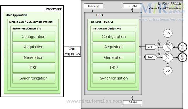
Figure 2. The architecture of the NIPXIe-5644R vector signal transceiver allows emulation and deployment of user-editable DSP blocks in the host or device firmware. Other input/output and memory interfaces can also be modified to complement the algorithm design.
The main factors of this migration and the main obstacles from the design of the algorithm to the final deployment (whether it is the design itself or the test) are the correct integration of the actual timing, and more importantly, the hardware I/O and signal calibration. For design and test functions, DSP algorithm designers often differ from teams that implement device firmware including I/O integration. With vector signal transceivers and LabVIEW RIO programmable devices, NI will offer a flexible programmable RF hardware platform that will include highly optimized IP blocks. The program block can manage the general complexity of high-speed A/D and D/A integrated with signal calibration, as well as DMA data flow to the host processor and high-speed on-board memory. The IP in this vector signal transceiver represents three main characteristics. You can first simulate the functionality in your desktop computer for use in algorithm design. The second source code can be used for reference or modification. As previously mentioned, a seamless migration to an actual real-time execution system can be supported in the end.
Integrated Design, Development, and Deployment In order to truly implement a tight system design flow from algorithm to deployment, a complete software/hardware perspective is required. The software must contain the correct timing, I/O, and DSP algorithm IP. The IP must be able to support simulation execution, and it needs to perform functional debugging quickly and support rapid design cycles, and eventually move test and design code from the desktop environment to programmable deployment hardware.
User-developed algorithms and tests are all important intellectual property (IP), and the main task of any system design tool is to maximize development efficiency, allowing the user to reuse the same IP when there is a small difference between the original design and the final implementation. This is only possible if the system design software initially used open and reusable building blocks for program implementation, and the basic building blocks are fully compatible with the reconfigurable hardware used for the iterative design process. This can be achieved by combining LabVIEW system design software and vector signal transceivers that support LabVIEW RIO.
Designed by professional hydraulic personnel ,which realized stability,durability,high efficiency,energy saving and low noise.
Neat oil,water and electric pipeline layout.
The reasonable structure is convenient for regulation and daily maintenance.
Adopt world famous brand of proportional valve,which accurately control actions of injections of injection,enabled the stable and reliable system operation.
Verification of many year's market application,optimal combination configuration.stable,reliable and durable system with the characteristics of high efficiency,energy saving,low noise and strong power.

Energy Saving Injection Moulding Machines
Energy Saving Injection Moulding Machines, Energy Saving Injection Machines ,Efficiency Energy Saving Injection,Energy Saving Plastic Injection
Ningbo Tongyong Plastic Machinery Manufacturering Co. Ltd. , http://www.tongyongmachinery.com