[Chinese instrument network instrument research and development] Recently, the Institute of Micro-nano Manufacturing and System Integration of the Chongqing Institute of Green Intelligent Technology of the Chinese Academy of Sciences in cooperation with the Chinese University of Hong Kong, the University of Electronic Science and Technology and Chongqing University of Technology, in situ growth of three-dimensional graphene based on the silicon surface Technically, research advances in obtaining high-performance heterojunction photodetectors have been published in the Nanoscale journal under the title High-performance Schottky heterojunction photodetector with fabricated nanoparticles as sensory electrodes.
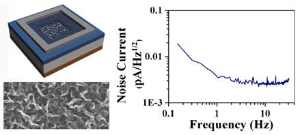
Graphene nanowall and its photodetector structure diagram and photodetector low noise current schematic
Schottky junction photodetectors using graphene as an electrode have the advantages of low dark current, fast response, and positive incidence. However, two-dimensional graphene films cannot be grown in-situ on a silicon-based substrate, and the formation of the graphene electrodes requires a wet or dry transfer process based on an organic support material, and the inevitable organic residue in the transfer process causes graphene. - Contamination of silicon heterojunction interface reduces the quality of the Schottky barrier, thereby affecting the photoelectric response of the photodetector; in addition, the residual metal catalyst required for the growth of the two-dimensional graphene film during the transfer process will also contribute to the device quality. Has an adverse effect. The three-dimensional graphene wall is a grid interconnection structure formed by longitudinally grown multilayer graphene, which retains the Raman characteristic peak of the graphene film; at the same time, the three-dimensional graphene can be grown in situ on the silicon substrate without metal catalysis. Avoid metal catalysts and organic residue contamination during the transfer process.
This research utilizes the ultra-clean silicon-graphene interface realized by in-situ growth of a three-dimensional graphene wall and realizes a high-performance photodetector. Experiments show that the Schottky junction ideal factor is less than 1.2, the detector's switching ratio is 2×10⁷, the responsivity is greater than 0.57A/W, the response time is less than 25ms, the 3dB cutoff frequency is greater than 8.5kHz, and the ratio of detection and calculation detection reaches respectively 5.88×1013 cm Hz1/2/W and 2.27×1014 cm Hz1/2/W. The study received funding support from the National Natural Science Foundation of China and the Chongqing Municipal Fundamental and Frontier Research Program.
(Original title: Chongqing Research Institute and other three-dimensional graphene heterojunction photodetector parts research progress)
WEIHAI SUNSHINE YACHTS CO.,LTD , https://www.ssboats.cn